927 views admin 2022-11-24
Entering the era of artificial intelligence and big data, the display device is no longer a simple information display screen, but an interactive, high-fidelity and immersive information interaction terminal. For the display device, it is possible to realize three-dimensional images in space, interactive, Energy saving, light and thin, flexible and foldable curling, super large size and other requirements. The entire technology and industrial chain of the display industry from materials, equipment, devices to manufacturing technology is entering a brand new revolution. Micro-LED display technology came into being. As players in the industry chain continue to increase their layout, it is very important who can crack the "key" of the new track to open up the technological precedent.
What are Micro LEDs?
Micro-LED display technology is a self-luminous display technology that integrates arrayed micron-scale LED light-emitting devices (μLEDs) on an active addressable drive substrate to achieve individual control and lighting to output display images. Micro-LED displays have many advantages such as self-illumination, high resolution, low response time, high integration, high reliability, etc., and are small in size, high in flexibility, easy to disassemble and merge, and can be applied to existing small-sized to large-scale In any display application of any size, and in many application scenarios, Micro-LED display can exert a better display effect than liquid crystal display (LCD) and organic light-emitting diode display (OLED).
Micro LED Epitaxy Technology Challenge
Although Micro-LED display technology is developing rapidly, due to the transformation of LED from lighting applications to display applications, it has raised higher requirements and challenges for LED epitaxy.
(1) Selection of substrate material
The choice of substrate material and epitaxy technology have a crucial impact on the performance of Micro-LED devices. Since Micro-LED chips are smaller than traditional chips to less than 50 μm, their extremely high yield and uniformity requirements pose higher requirements and challenges for substrate selection and epitaxy technology. When applied to high-resolution display, the injection current density of Micro-LED is very low, and the non-radiative recombination caused by defects is particularly prominent, which greatly reduces the light output efficiency of Micro-LED, so for Micro-LED, lower defect density is required epitaxial wafers.
At present, the substrates that can be commercially used on a large scale include sapphire, SiC and Si substrates, but using these substrates as GaN epitaxy is heterogeneous epitaxy, due to the lattice mismatch and thermal mismatch between the heterogeneous substrate and the GaN epitaxial layer matching, so that the dislocation density of the epitaxial layer is higher. Compared with heterogeneous substrates such as sapphire, SiC and Si, the choice of GaN material as the substrate can greatly improve the crystal quality of the epitaxial wafer, reduce the dislocation density, and improve the working life, luminous efficiency and working current density of the device. However, it is very difficult to prepare GaN single crystal substrates, the price of GaN substrates is very expensive, and the maximum size is only 4 inches (10.16 cm), so it is difficult to meet the needs of commercialization.
(2) Wavelength Uniformity Control
Micro-LED display technology is a self-luminous display technology. In high-resolution display applications, the difference in color rendering caused by the uneven emission wavelength of Micro-LEDs will greatly affect the display effect. In order to ensure the display effect, the standard deviation of the wavelength variation of a single Micro-LED epitaxial wafer needs to be controlled at 0.8 nm or less. Therefore, the control of gas flow and temperature uniformity is particularly important during the epitaxial growth of InGaN/GaN quantum wells by metal organic chemical vapor deposition (MOCVD).
Optimizing the gas flow uniformity in the MOCVD epitaxial growth process plays a vital role in improving the LED wavelength uniformity. At present, Prismo UniMax, the latest domestic medium and micro MOCVD equipment, adopts partition temperature control technology to ensure the balance of the entire temperature field during epitaxial growth. At the same time, it uses a series of strain control technologies such as MO source and air flow uniformity to improve the wavelength uniformity of LED epitaxial wafers. To meet the needs of Micro-LED display. For the high requirements of wavelength uniformity in Micro-LED applications, the design of the graphite tray can be optimized so that it has a certain curvature to better match the warpage of the epitaxial wafer during the epitaxial growth process and has achieved further improvement in the control of temperature uniformity.
(3) Defect control
Dislocations as non-radiative recombination centers and leakage channels will significantly affect the performance of chip Micro-LEDs. Due to the small size and low injection current density of Micro-LEDs, their optoelectronic properties are very sensitive to dislocation density. At present, patterned substrate technology, buffer layer technology, etc. are more widely used in heteroepitaxial growth of GaN on sapphire or silicon substrates to reduce dislocation density and improve crystal quality. The homoepitaxial technology of high-quality GaN substrate can effectively reduce the dislocation density of LED epitaxial wafers.
The Nanchang University team improved the quality of the silicon substrate LED epitaxial layer by optimizing the AlN buffer layer and the superlattice insertion layer filtering dislocation technology on the silicon substrate. Its epitaxial structure and external quantum efficiency curves are shown in Fig. 3(a) and (b). Through this method, the external quantum efficiency (EQE) of the luminous wavelength 551 nm LED was increased to 37.7% (4A/cm2). Continue to use defects to introduce V-shaped pits to greatly increase the In composition and improve crystal quality. The V-shaped pits make the active region change from a traditional planar structure to a three-dimensional structure. In addition to the original vertical p-n junction, a horizontal p-n junction is introduced. Coordinating the two can control the carrier transport path as well as the recombination location, thereby enhancing LED performance. Figure (c) below shows the cross-sectional view of a typical V-shaped pit and the transport path and recombination position of carriers near the V-shaped pit.
From ordinary LED lighting to Mini-LED display, and then to Micro-LED display, the chip size is continuously shrinking, and the difficulties brought about are also increasing. Micro-LED not only needs a breakthrough in epitaxy technology, but also the upgrading of MOCVD equipment is equally important. At present, Micro-LED is constrained by cost and yield rate. Looking forward to the future, there is still a long way to go for the large-scale commercialization of Micro-LED.
more articles:
Technology | What are the advantages and disadvantages of COB display packaging technology
Sunrise LED Display manufacturer
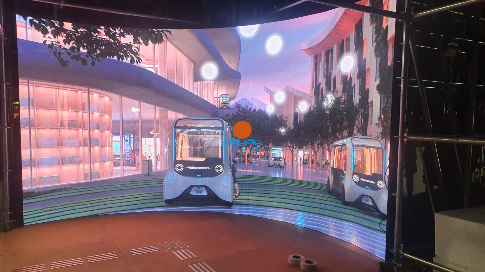
At present, the naked eye 3D large screen market is hot, and 3D technology is also known as 3D di...
Sunrise’s p2.604 curved LED display lights up under the Eiffel Tower Sunri...

Concert activities are popular in the United States, and sunrise’s products have been wide...

Sunrise 264 square meters Galaxy 3115 series mesh led facade in Armenia Sun...
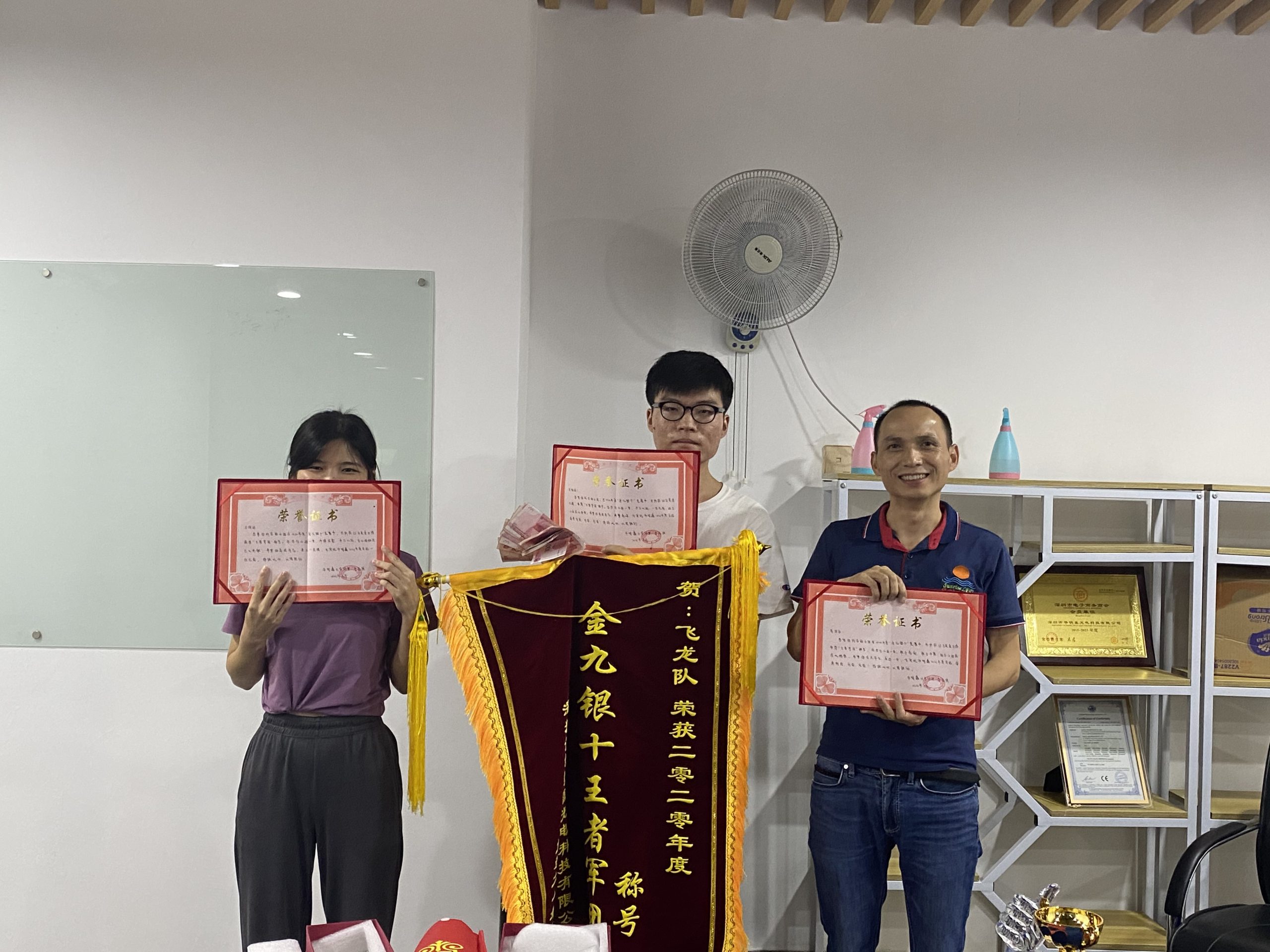
Doris, as a new salesman, won three orders in two months. It’s great. Jack, the bu...
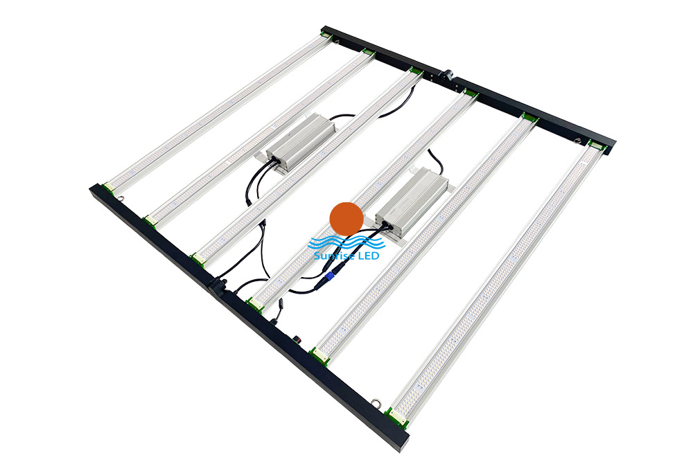
640w and 800W full spectrum led grow light It can be folded for convenient transportatio...
The latest project, Saudi Arabia LED MESH FACADE. Ultra-high brightness, ultra-light LED display ...