news

Study on improving light extraction rate of far-ultraviolet LED by using gallium nitride

101 views admin 2023-09-21

  • Silanna UV-A research team has published research using the properties of gallium nitride: Aluminum nitride (GaN: AlN) short-period superlattice (SPSL), claiming a record radiation flux of 17.4mW for a Far-C UV LED grown on sapphire
  • 01
  • AlGaN LED is the way to achieve low cost, compact UV light source While AlGaN leds are seen as a way to achieve low-cost, compact UV light sources, there are still many challenges to overcome. As the aluminum content of AlGaN increases, the resulting light becomes more difficult to extract because the recombination process emits photons into the transverse magnetic (TM) mode instead of the transverse electrical (TE) mode. As a result, the light is mainly emitted parallel rather than perpendicular to the device layer, and another problem with high aluminum-content AlGaN is low doping efficiency.
  • In GaN, the light emission tends to be perpendicular to the device layer, the heavy hole (HH) band is the highest energy level, and the electrons in the conduction band are mainly reorganized here. In contrast, in the high aluminum-content AlGaN, the energy level of the field splitting hole (CH) band is the highest, and electrons reassembled into this band emit a TM mode.
  • Figure 1: Valence band energy-quantity (E-k) diagrams of (a) massive Al0.8Ga0.2N and (b) 1:4 monolayer GaN:AlN short-period superlattice (SPSL) (period L) along the C-axis calculated using 6x6 k.p theory.
  • 02
  • Different LED target wavelengths can be obtained by changing the thickness of SPSL layer
  • To this end, the Silanna UV team used the SPSL structure to restore the HH small band (HH1) to the highest energy level, thus achieving TE light extraction. In addition, SPSL can also alleviate doping efficiency issues, and the research team used SPSL not only to replace one part of the device structure, but to use SPSL in almost the entire epitaxial material layer.
  • It is understood that the AlN:GaN short-period superlattice (SPSL) LED material was grown on a 6-inch sapphire substrate by plasma-assisted molecular beam epitaxy (PAMBE) technology (Figure 2). There is an artificial strain between the material and the underlying 400nm AlN buffer layer.
  • Figure 2: (a) Basic device structure of SPSL UV LED. (b) Transmission electron microscope images of the interface between the recombination region and the chirped region. (c) X-ray diffraction X-ray 2h scan of SPSL growing on the AlN buffer.
  • It can be seen from the figure that SPSL is alternately composed of GaN layer and AlN layer. By changing the thickness of these layers, the effective aluminum content of different group III nitride materials can be obtained, so as to obtain different LED target wavelengths.
 
  • 03
 
  • The use of the SPSL structure can reduce the resistivity by three times
  • Silanna UV's team tested the device, whose 80nm/ 36-cycle recombination region and 450nm bulk N-type region are separated by a 50nm high-conductivity region with a low aluminum content of 1:4 single-layer GaN: aluminum nitride, resulting in an effective aluminum content of 80% over 37 cycles. The use of SPSL structures can reduce the resistivity by a factor of three, which is similar to the resistivity value reported for bulk Al0.8G0.2N materials. For 229-240 nm wavelengths, the aluminum content in the reconstituted/high-volume region is about 93-98%.
  • In addition, the final region of the device includes a chirped/graded layer of 20 nm, which transitions to a P-type GaN cover layer of 40 nm as the GaN layer thickness increases.
  • According to the research team, the chirped layer is intended to improve hole injection from the lower band gap GaN to the SPSL recombination region, and also acts as an electron barrier layer, limiting electrons from crossing the recombination layer.
  • At the same time, the ionizing receptor concentration in the cap was about 1x10¹⁹/cm3, and the ionizing donor concentration in the high-conductivity SPSL layer was estimated to be 8x10¹⁹/cm3. This material is made into passivated Mesa leds with titanium/aluminum contacts. Photoelectric measurements are made via a 2-inch integrating sphere at the bottom of the wafer. The wavelength and power performance of the device are uniform across the entire chip. However, the electrical properties are not so uniform. "This is because the series resistance, as well as the electrical properties, are affected by the etching and metallization processes, not just the MBE growth processes," the research team explains.
  • It states that a chip with 233 ±1nm wavelength devices can produce 10,763 leds. The 4-inch wavelength standard deviation inside the chip is only 0.16 nanometers. At 20mA injection, the average optical power output of this inner part is 0.2W. For devices more than half an inch from the edge of the chip, the 20 mah drive voltage standard deviation is less than 0.16 volts.
  • According to the research team, "It is possible to produce areas larger than 4 inches with consistent performance, and the MBE growth SPSL LED method is one of the most promising methods from the point of view of production volume and yield."
  • 04
 
  • Reach the highest radiation flux of Far-C LED, 1A time output of 17.4mW
  • The research team also used the electrostatic discharge protection function of a commercial Zener diode shunt to package a 1mmx1mm single crystal LED. The thickness of the LED was reduced to 275μm before being encapsulated in an aluminum nitride ceramic material, and measurements were made in a 6-inch integrating sphere (Figure 3).
  • Figure 3: (a) Typical optical output power, wall insertion efficiency, and voltage vs. injection current for a device with a wavelength of 236nm. (b) The lifetime performance of a single device at a continuous current of 20mA for 3,000 hours according to TM21. (c) R70 percentile for 80 packaged devices.
 
  • Experiments show that a typical package device has a wall insertion efficiency of 0.55% at 50mA injection, a radiation flux of 1.7mW at 0.55% peak efficiency, and a light output of 17.4mW at 1A. "While this greatly exceeds the predetermined drive current, it is the highest radiation flux reported for an ultra-ultraviolet LED grown on a sapphire substrate," the team said.
 

Technology | analysis of naked eye 3D display technology

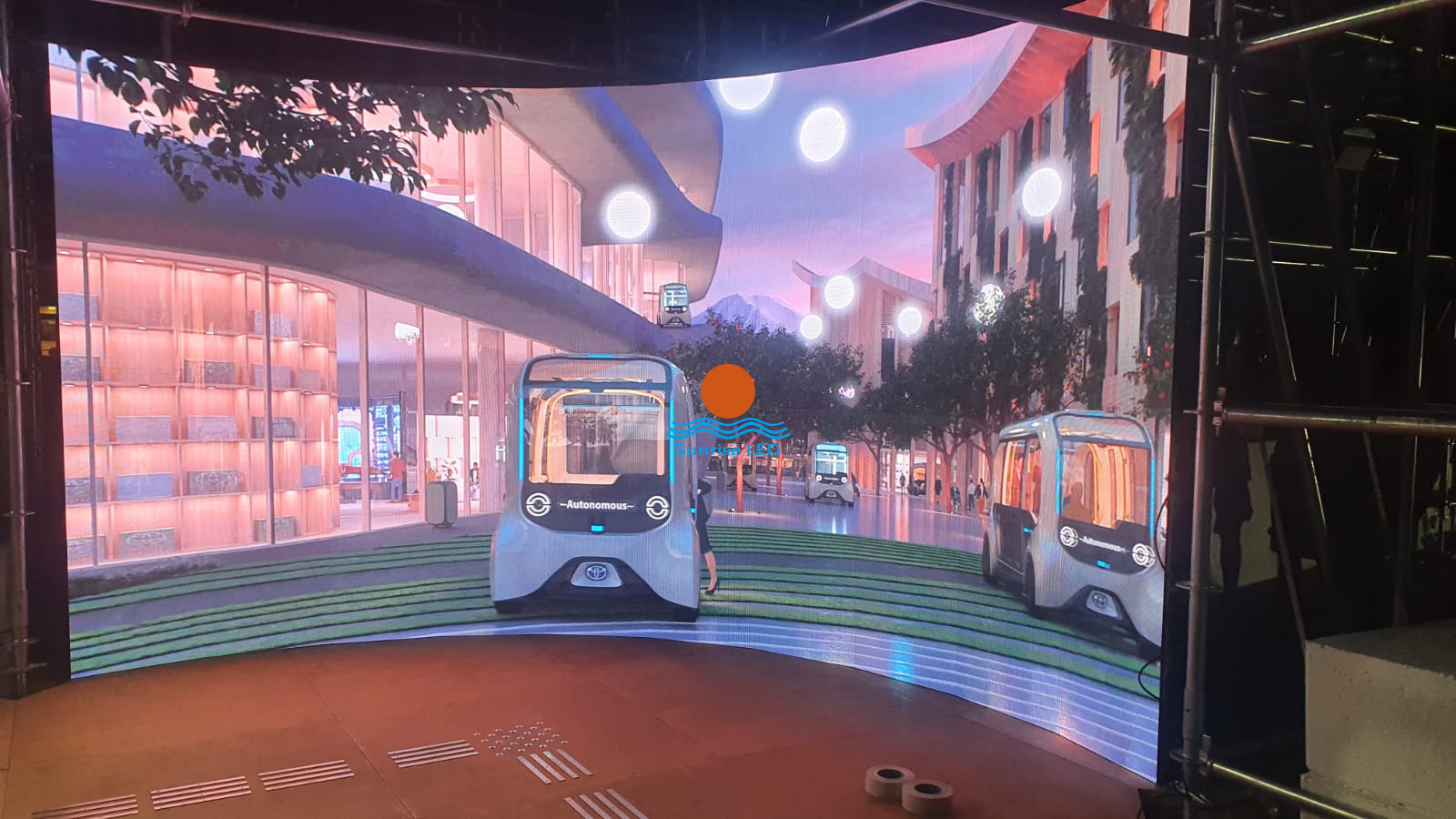
At present, the naked eye 3D large screen market is hot, and 3D technology is also known as 3D di...

Do you like ?955 views

Read more

Sunrise’s p2.604 curved LED display lights up under the Eiffel Tower

Sunrise’s p2.604 curved LED display lights up under the Eiffel Tower     Sunri...

Do you like ?756 views

Read more

Sunrise LED Rocky Rental Series led display for concert

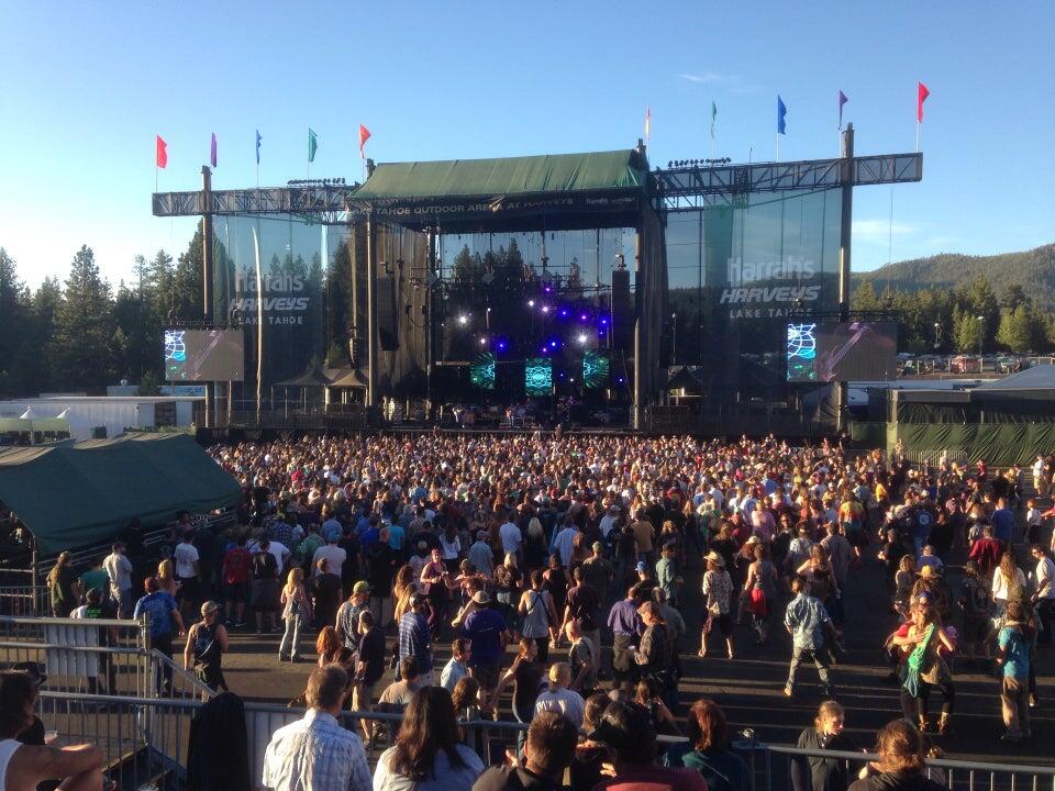
Concert activities are popular in the United States, and sunrise’s products have been wide...

Do you like ?1,177 views

Read more

Sunrise 264 square meters Galaxy 3115 series mesh led facade in Armenia

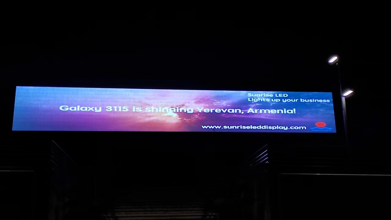
  Sunrise 264 square meters Galaxy 3115 series mesh led facade in Armenia     Sun...

Do you like ?960 views

Read more

Sunrise led presents awards to excellent salesmen!

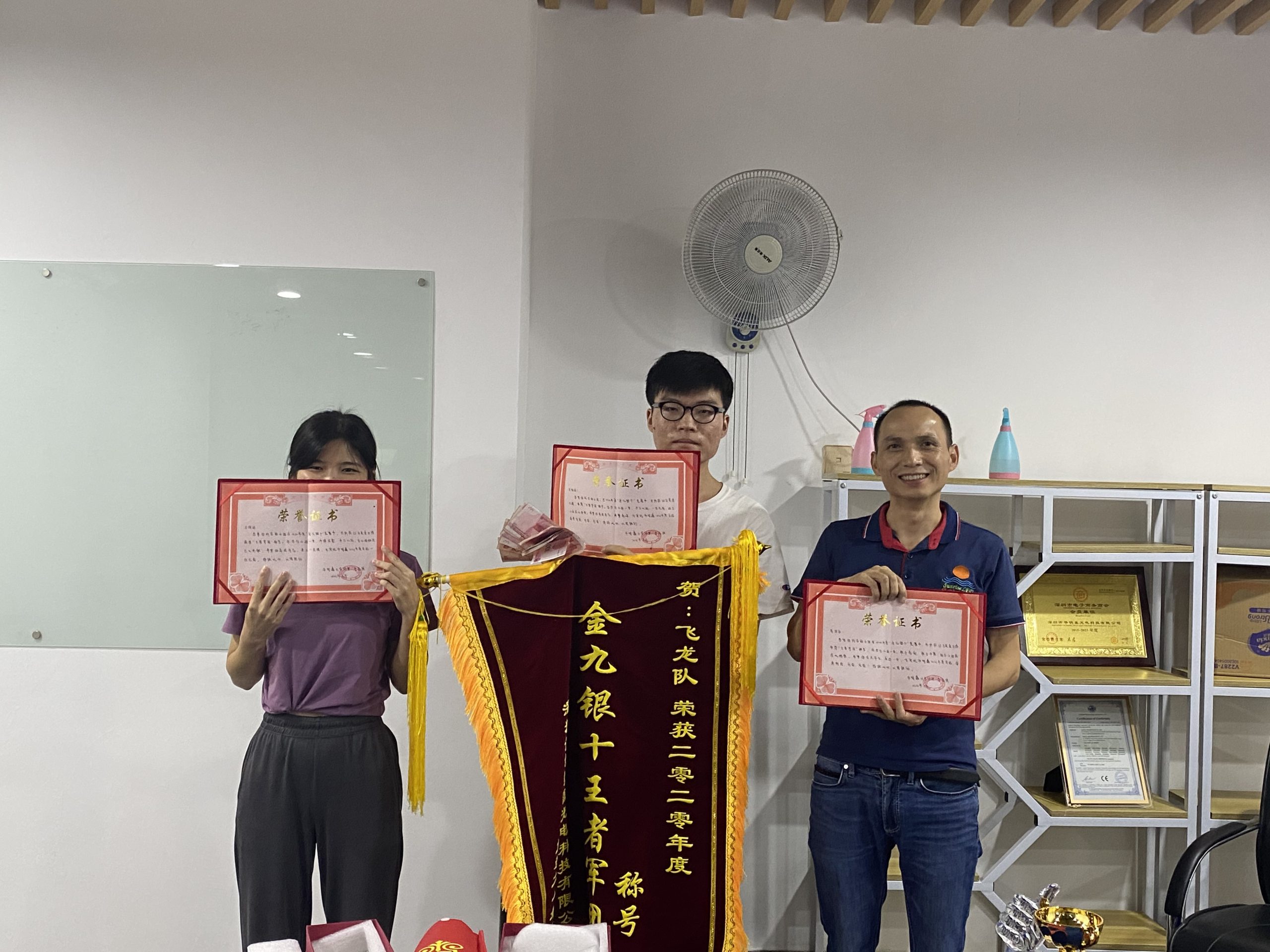
Doris, as a new salesman, won three orders in two months. It’s great.   Jack, the bu...

Do you like ?794 views

Read more

Our new product, led grow light, PPE reaches 2.6umol/j

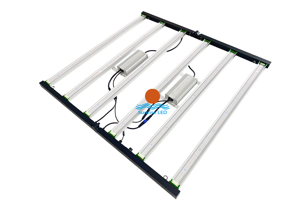
640w and 800W full spectrum led grow light   It can be folded for convenient transportatio...

Do you like ?748 views

Read more

The latest project, Saudi Arabia LED MESH FACADE

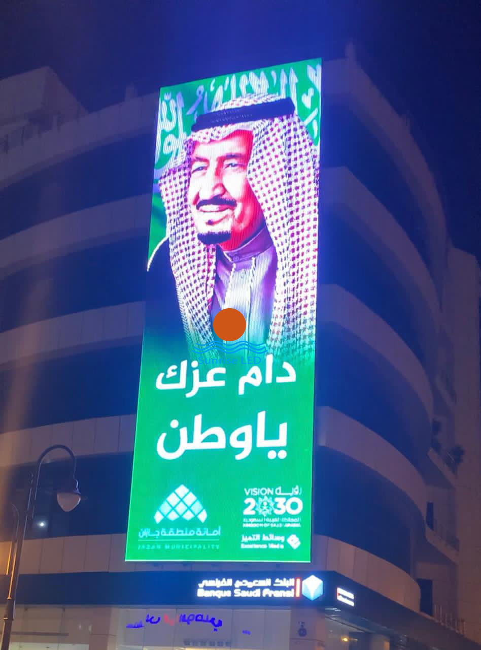
The latest project, Saudi Arabia LED MESH FACADE. Ultra-high brightness, ultra-light LED display ...

Do you like ?1,256 views

Read more
Technical Support: Magic Lamp