995 views admin 2021-07-06
With the development of LED technology, from large space outdoor products to indoor close viewing LED display screen, the application in indoor is more and more common. Especially with the rapid development of smart city and security industry, and the development of digital enterprises and digital era, the demand for indoor display hardware is increasing.
Development history of interior display products
Since 2015, the localization rate of MOCVD has increased rapidly, the capacity of LED chip has been released rapidly, and the chip price has decreased, which has effectively reduced the price of LED lamp beads. Mature technology makes the package size of lamp beads smaller and smaller, which promotes the development of the industry.
Small space led category increased, and began to compete with DLP and LCD indoor display market. From the data of global LED display market scale, from 2018 to 2022, the performance advantages of small spacing LED display products are obvious, forming a trend of replacing traditional LCD and DLP technologies.
Industry distribution of small space led customers
In recent years, small spacing LED has achieved rapid development, but due to cost and technical problems, it is mainly used in the field of professional display. These industries are not sensitive to product price, but have relatively high requirements for display quality, so they quickly occupy the market in the field of professional display.
Development of small space led from special display market to commercial and civil market
After 2018, with the maturity of technology and the decrease of cost, small space LED will break out in the commercial display market such as conference rooms, education, shopping malls and cinemas. Overseas market demand for high-end small spacing LED is accelerating. Among the top 8 LED manufacturers in the world, 7 are from China, and the top 8 occupy 50.2% of the global market share. I believe that with COVID-19's stability, the overseas market will soon pick up.
Analysis of small space LED packaging technology
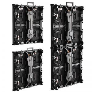
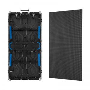
SMD is the abbreviation of surface mount device. The bare chip is fixed on the bracket, and the positive and negative electrodes are electrically connected through metal wires. The SMD LED lamp beads are made by using epoxy resin for protection. The LED lamp beads are welded with PCB by reflow soldering to form the display unit module, and then the module is installed on the fixed box, equipped with power supply and PCB The control card and wire form the LED display.
Compared with other packaging situations, SMD packaging products have more advantages than disadvantages, which are in line with the characteristics of domestic market demand (decision-making, procurement, use). It is also the mainstream products in the industry, and can get service response quickly.
Cob process is that led chips are directly adhered to PCB with conductive or non-conductive adhesive, and wire bonding is used to realize electrical connection (front mounting process) or chip flip chip technology (without metal wire) is used to directly connect the positive and negative poles of lamp beads with PCB (flip chip process), and finally the display unit module is formed, and then the module is installed on the fixed box, equipped with power supply The control card and wire form the LED display. Cob technology has the advantages of simplifying the production process, reducing the cost of the product and reducing the power consumption. Therefore, the display surface temperature is reduced and the contrast is greatly improved. Its disadvantages are that the reliability is faced with greater challenges, the lamp repair is difficult, and the brightness, color and ink color are difficult to achieve consistency.
IMD is to package n groups of RGB lamp beads in a small unit to form a lamp bead. The main technical routes are: 4 in 1 for Gongyang, 2 in 1 for Gongyin, 4 in 1 for Gongyin, 6 in 1 for Gongyin, etc. The advantage of integrated packaging is that the size of lamp beads is larger, the surface mounting is easier, the distance between dots is smaller, and the maintenance difficulty is reduced. The disadvantage is that the current industrial chain is not perfect, the price is higher, the reliability is facing greater challenges, the maintenance is not convenient, the consistency of brightness, color and ink color has not been solved, and it needs to be further improved.
Micro LED is a technology that transfers a large amount of address of traditional LED array and miniaturization to the circuit board to form ultra-small spacing led, and further miniaturizes the length of millimeter level led to micron level, so as to achieve ultra-high pixel and ultra-high resolution. Theoretically, it can adapt to the technology of screen of various sizes. At present, in the bottleneck of micro led, the key technology is to break through the micro process technology and mass transfer technology. Secondly, the film transfer technology can break through the size limit to complete batch transfer, which is expected to reduce the cost.
Gob is an integral surface coating technology for surface mount module. It is a transparent colloid on the surface of traditional SMD small spacing module to solve the problem of strength and protection. In essence, it is SMD small spacing product. Its advantages lie in reducing the dead lamp rate, increasing the anti-collision strength and surface protection of lamp beads. Its disadvantages lie in the difficulty of repairing lamp, module deformation and reflection caused by colloid stress, It is characterized by local degumming, colloidal discoloration and difficult repair of false welding.
AOB is a surface mount module bottom coating technology, and it also encapsulates half layer transparent colloid in the lamp bead gap of traditional SMD small spacing module to solve the protection problem. In essence, AOB is SMD small spacing product, which has limitations and potential risks. For example, it is difficult to achieve the gap below p1.25, only top lamp beads can be used, and the potential problems of surface mount process still exist.
Cog package is that the chip is directly bound to the glass by conductive adhesive. The advantages are that the volume and weight of the display panel are greatly reduced, and it is easy to mass produce, but there are certain limitations and potential risks, such as the glass substrate is limited by size, which is suitable for small area application, and temporarily not suitable for large area splicing.
more articles:
Technology | summer is coming, how to heat the LED screen?Sunrise LED Display manufacturer
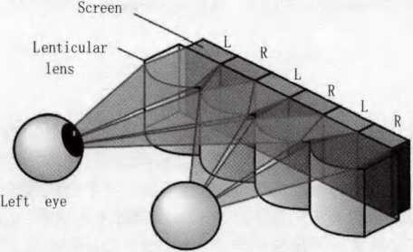
At present, the naked eye 3D large screen market is hot, and 3D technology is also known as 3D di...
Sunrise’s p2.604 curved LED display lights up under the Eiffel Tower Sunri...

Concert activities are popular in the United States, and sunrise’s products have been wide...
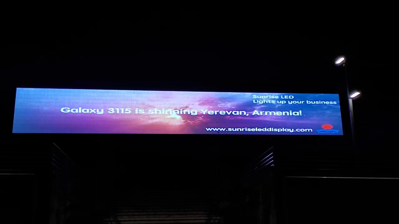
Sunrise 264 square meters Galaxy 3115 series mesh led facade in Armenia Sun...
Doris, as a new salesman, won three orders in two months. It’s great. Jack, the bu...
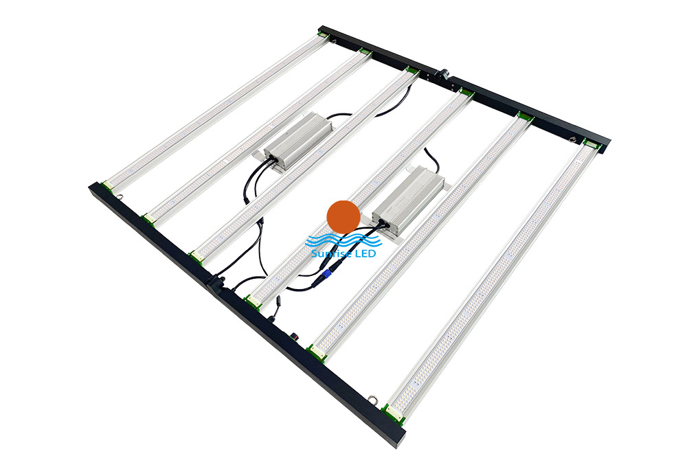
640w and 800W full spectrum led grow light It can be folded for convenient transportatio...
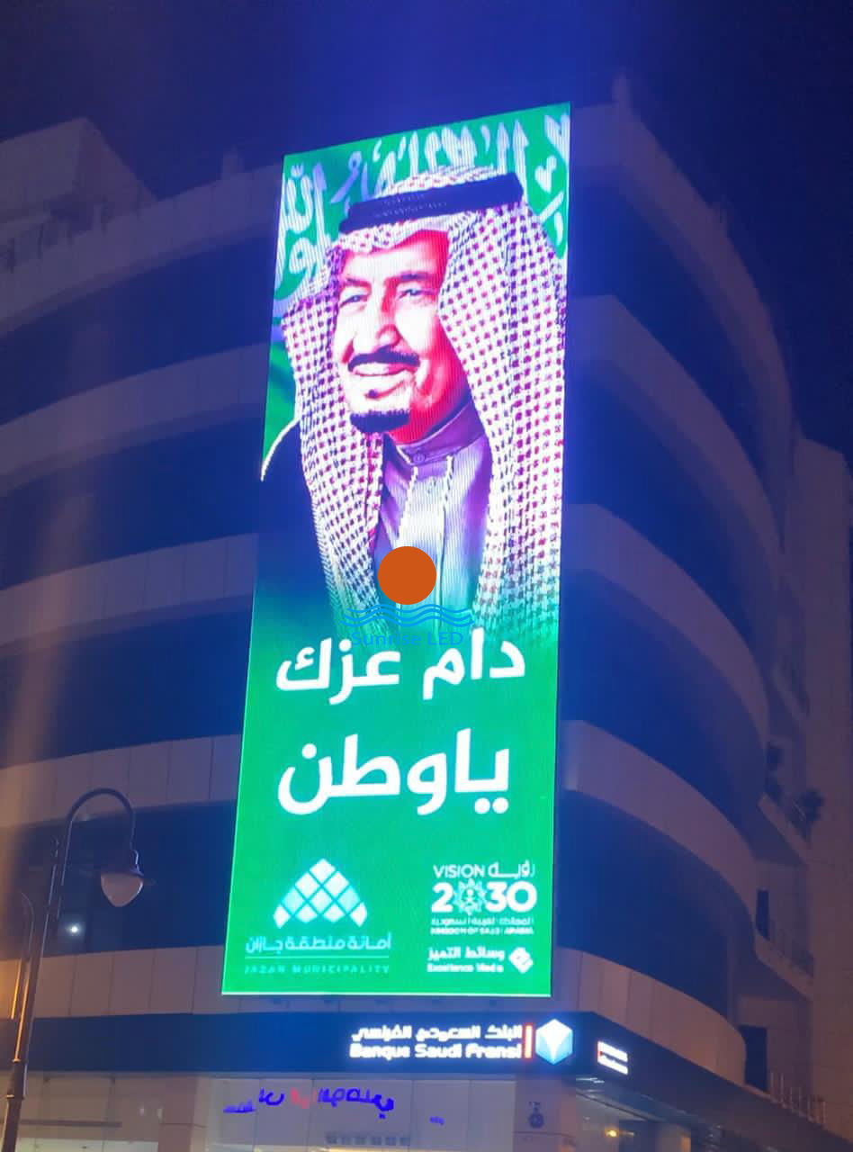
The latest project, Saudi Arabia LED MESH FACADE. Ultra-high brightness, ultra-light LED display ...