news

Packaging technology small pitch LED analysis

100 views admin 2023-11-17

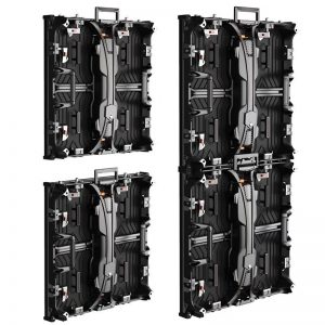
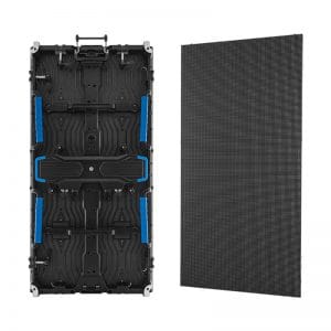
  • SMD stands for Surface Mount Device. The bare chip is fixed on the bracket, electrically connected between the positive and negative electrodes through a metal wire, protected by epoxy resin, and made into an SMD led lamp bead. After the led lamp bead is reflow welded with the PCB, the display unit module is formed, and then the module is installed on the fixed box, equipped with the power supply, control card and wire, and the finished LED display is formed.
  • Compared with other packaging situations, SMD packaging products have more advantages than disadvantages, meet the requirements of the domestic market (decision-making, purchase, use), and are also mainstream products in the industry, which can quickly get a service response.
  • The COB process is to glue the LED chip directly on the PCB with conductive or non-conductive adhesive, and then perform lead bonding to achieve electrical connection (formal process), or use flip chip technology (no metal wire) to connect the positive and negative electrodes of the lamp bead directly with the PCB (flip process), and form a display module finally.
  • Then the module is installed on the fixed box, equipped with a power supply, control card and wire to form the finished led display. COB technology has the advantages of simplifying production process, reducing product cost and power consumption, reducing the surface temperature of the display and greatly improving the contrast. The disadvantage is that the reliability faces greater challenges, the repair of the lamp is difficult, and the brightness, color, and ink color are difficult to achieve consistency.
  • IMD integrates n sets of RGB lamp beads into a small unit to form a lamp bead. Main technical routes: Yang Gong 4 in 1, Gongyin 2 in 1, Gongyin 4 in 1, Gongyin 6 in 1, etc. The advantages of the integrated package are that the lamp bead size is larger, easier to surface mount, the point spacing is smaller, and the maintenance is less difficult. The disadvantage is that the current industrial chain is not perfect, the price is high, the reliability is facing greater challenges, the maintenance is not convenient, the consistency of brightness, color and ink color is not solved, and it needs to be further improved.
  • Micro LED is a technology that transfers the traditional LED array and miniaturization to the circuit board to form an ultra-small-pitch LED, further miniaturizing the length of the millimeter-level LED to the micron level, thus achieving ultra-high pixels and ultra-high resolution, which can theoretically adapt to various sizes of screens. At present, in the bottleneck of micro-LED, the key technology is to break through micro-processing technology and huge transfer technology. Secondly, film transfer technology can break through the size limit to complete batch transfer, which is expected to reduce costs.
  • GOB is the integral surface coating technology of surface mount modules, which encapsulates a layer of transparent colloid on the surface of traditional SMD small-pitch modules to solve the problems of strength and protection. It is essentially an SMD small pitch product. Its advantage is to reduce the dead lamp rate, increase the anti-knock strength and surface protection of the lamp bead. The disadvantage is that the lamp is difficult to repair, the colloidal force leads to module deformation, reflection, partial degumming, colloidal discoloration, and virtual welding repair.
  • AOB is the glue technology at the bottom of the surface paste module, and a half layer of transparent glue is also encapsulated in the gap of the traditional SMD small-pitch module lamp beads to solve the protection problem. In essence, AOBs are SMD small distance products with limitations and potential risks. For example, the gap below P1.25 is difficult to do, only the top lamp bead can be used, and the potential problems of surface mount technology still exist.
  • The COG package is a chip directly bound to the glass by a conductive adhesive. It has the advantages of greatly reducing the size and weight of the display panel and easy mass production. However, there are also certain limitations and potential risks, such as because the glass substrate size is limited, suitable for small area applications are temporarily not suitable for large area splicing.

Technology | analysis of naked eye 3D display technology

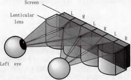
At present, the naked eye 3D large screen market is hot, and 3D technology is also known as 3D di...

Do you like ?973 views

Read more

Sunrise’s p2.604 curved LED display lights up under the Eiffel Tower

Sunrise’s p2.604 curved LED display lights up under the Eiffel Tower     Sunri...

Do you like ?773 views

Read more

Sunrise LED Rocky Rental Series led display for concert

Concert activities are popular in the United States, and sunrise’s products have been wide...

Do you like ?1,195 views

Read more

Sunrise 264 square meters Galaxy 3115 series mesh led facade in Armenia

  Sunrise 264 square meters Galaxy 3115 series mesh led facade in Armenia     Sun...

Do you like ?966 views

Read more

Sunrise led presents awards to excellent salesmen!

Doris, as a new salesman, won three orders in two months. It’s great.   Jack, the bu...

Do you like ?797 views

Read more

Our new product, led grow light, PPE reaches 2.6umol/j

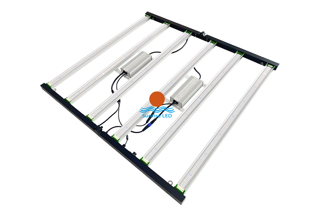
640w and 800W full spectrum led grow light   It can be folded for convenient transportatio...

Do you like ?751 views

Read more

The latest project, Saudi Arabia LED MESH FACADE

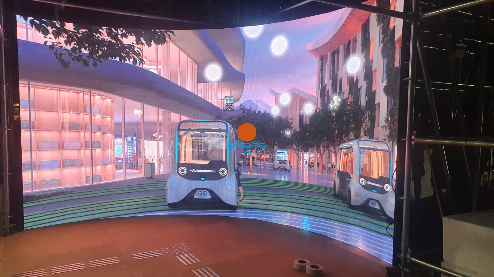
The latest project, Saudi Arabia LED MESH FACADE. Ultra-high brightness, ultra-light LED display ...

Do you like ?1,258 views

Read more
Technical Support: Magic Lamp